National Institute of Technology, Calicut

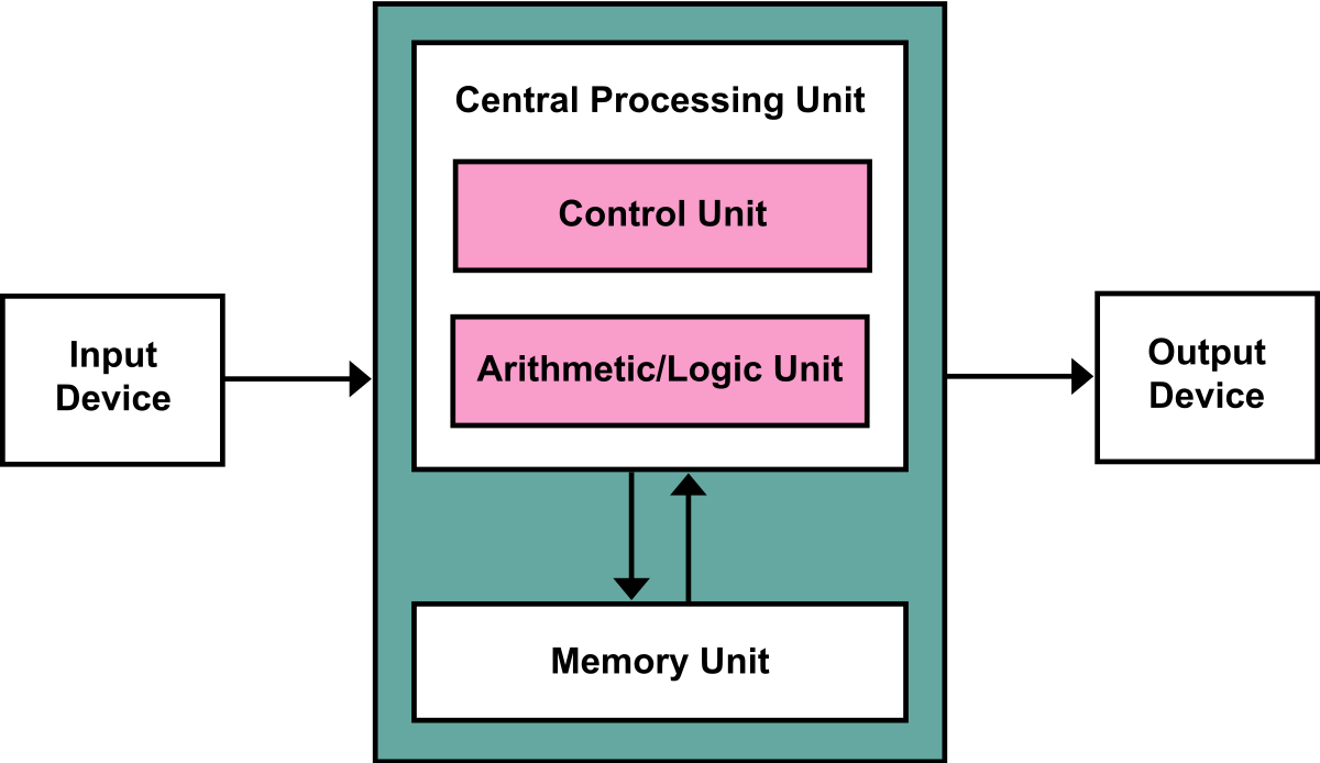
Von Neumann Architecture
Intel Core i9
What is a clock cycle?
Intel maintains its backward compatibility of instruction sets, i.e, we can run a program designed for an old 16 bit machine in a 32bit machine. That is the reason why we can install 32-bit OS in a 64 bit PC. The only problem is that, the program will not use the complete set of registers and other available resources and thus it will be less efficient.
A register may hold an instruction, a storage address, or any kind of data (such as a bit sequence or individual characters). A register must be large enough to hold an instruction - for example, in a 64-bit computer, a register must be 64 bits in length.General purpose registers are used to store temporary data within the microprocessor.There are eight general purpose registers. They are EAX, EBX, ECX, EDX, EBP, ESI, EDI, ESP. We can refer to the lower 8 and 16 bits of these registers (see image). This is to maintain the backward compatibility of instruction sets. These registers are also known as scratchpad area as they are used by the processor to store intermediate values in a calculation and also for storing address loca- tions.
The General Purpose Registers are used for :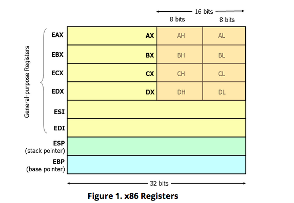
 EIP:
EIP:When we start a program, it will be copied into the main memory and EIP is the pointer which points to the starting of this program in memory and execute each instruction sequentially. Branch statements like JMP, RET, CALL, JNZ (we will see shortly) alter the value of EIP.
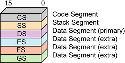
In x86 processors for accessing the memory basically there are two types of registers used Segment Register and Offset. Segment register contains the base address of a particular data section and Offset will contain how many bytes should be displaced from the segment register to access the particular data. CS contains the base address of Code Segment and EIP is the offset. It keeps on updating while executing each instruction. SS or Stack Segment contains the address of top most part of system stack. ESP and EBP will be the offset for that. Stack is a data structure that follows LIFO ie. Last-In-First-Out. There are two main operations associated with stack: push and pop. If we need to insert an element into a stack, we will push it and when we give the pop instruction, we will get the last value which we have pushed. Stack grows downward. So SP will always points to the top of stack and if we push an element, ESP (Stack Pointer) will get reduced by sufficient number of bytes and the data to be stored will be pushed over there. DS, ES, FS and GS acts as base registers for a lot of data operations like array addressing, string operations etc. ESI, EDI and EBX can act as offsets for them. Unlike other registers, Segment registers are still 16 bit wide in 32-bit processors.
In modern 32 bit processor the segment address will be just an entry into a descriptor table in memory and using the offset it will get the exact memory locations through some manipulations. This is called segmentation. Here in the memory ,the Stack Segment starts from the memory location 122 and grows downwards. Here the Stack Pointer ESP is pointing to the location 119. Now if we pop 1 byte of data from stack, we will get (01010101)2 and the ESP will get increased by one. Now suppose we have (01101100 11001111)2 in the register ax and we execute the push command:
push axThen the ESP will get reduced by two units (because we need two store two bytes of data) and ax will be copied over there: Here we can see that now ESP points to the lower byte of data from the 2 bytes data which we have pushed. In x86 architecture when we push or save some data in memory, the lower bytes of it will be addressed immediately and thus it is said to follow Little Endian Form. MIPS architecture follows Big Endian Form.
Endianness refers to the sequential order in which bytes are arranged into larger numerical values when stored in memory or when transmitted over digital links. Endianness is of interest in computer science because two con- flicting and incompatible formats are in common use: words may be repre- sented in big-endian or little-endian format, depending on whether bits or bytes or other components are ordered from the big end (most significant bit) or the little end (least significant bit).
Big Endian Byte Order:The most significant byte (the "big end") of the data is placed at the byte with the lowest address. The rest of the data is placed in order in the next three bytes in memory.
Little Endian Byte Order:The least significant byte (the "little end") of the data is placed at the byte with the lowest address. The rest of the data is placed in order in the next three bytes in memory.
Suppose an integer is stored as 4 bytes(32-bits), then a variable y with value 0x01234567( Hexa-decimal representation) is stored as four bytes 0x01, 0x23, 0x45, 0x67, on Big-endian while on Little-Endian (Intel x86), it will be stored in reverse order:

Bus is a name given to any communication medium, that transfers data between two components. (A bus is a subsystem that is used to connect computer components and transfer data between them.)A bus may be parallel or serial. Parallel buses transmit data across multiple wires. Serial buses transmit data in bit-serial format. We can classify the buses associated with the processor into three.
It is the bus used to transfer data between the processor and memory or any other I/O devices (for both reading and writing). As the size of data bus increases, it can transfer more data in a single stretch. The size of data bus in common processors by Intel are given below.
| Processor | Bus size |
|---|---|
| 8088, 80188 | 8 bit |
| 8086, 80816, 80286, 80386SX | 16 bit |
| 80386DX, 80486 | 32 bit |
| 80586, Pentium Pro and later processors | 64 bit |
The address bus is used by the CPU or a direct memory access (DMA) enabled device to locate the physical address to communicate read/write commands. Memory management Unit (MMU) or Memory Control Circuitry (MCC) or Memory Control Unit (MCU) is the set of elec- tronic circuits present in the motherboard which helps the processor in reading or writing the data to or from a location in the RAM. All address buses are read and written by the CPU in the form of bits.An address bus is measured by the amount of memory a system can re- trieve. A system with a 32-bit address bus can address 4 gigabytes of memory space.
The maximum size of RAM which can be used in a PC is determined by the size of the address bus. If the size of address bus is n bits, it can address a maximum of 2n bytes of RAM. This is the reason why even if we add more than 4 GB of RAM in a 32 bit PC, we cannot find more than 4 GB of available memory.
| Processor | Address Bus Width | Maximum Addressable RAM size |
|---|---|---|
| 8088, 8086, 80186, 80286, 80188 | 20 | 16 KB |
| 80386SX, 80286 | 24 | 16 MB |
| 80486, 80386DX, Pentium,Pentium Override | 32 | 4 GB |
| Pentium II, Pentium Pro | 36 | 64 GB |
For example, the data bus is used for both reading and writing purpose and how is it that the Memory or MMU knows the data has to be writ- ten to a location or has to be read from a location, when it encounters an address in the address bus? This ambiguity is being cleared using read and write bits in the control bus. When the read bit is enabled, the data in the EDB (external data bus or simply data bus) will be written to that location. When the write bit is enabled, MMU will write the data in the EDB into the address location in the address bus.
Interrupts are the most critical routines executed by a processor. Interrupts may be triggered by external sources or due to internal operations.
In linux based systems 80h is the interrupt number for OS generated in- terrupts and in windows based systems it is 21h. The Operating System Interrupt is used for implementing systems calls.
Whenever an interrupt occurs, processor will stop its present work, preserve the values in registers into memory and then execute the ISR (Interrupt Service Routine) by referring to an interrupt vector table. ISR is the set of instructions to be executed when an interrupt occurs. By referring to the interrupt vector table, the processor can get which ISR it should execute for the given interrupt.After executing the ISR, processor will restore the registers to its previous state and continue the process that it was executing before. Almost all the I/O devices work by utilizing the interrupt requests.
An interrupt is a signal from a device, such as the keyboard, to the CPU, telling processor to immediately stop whatever it is currently doing and do something else. For example, the keyboard controller sends an interrupt when a key is pressed. To know how to call on the kernel when a specific interrupt arise, the CPU has a vector table setup by the OS, and stored in memory. There are 256 interrupt vectors on x86 CPUs, numbered from 0 to 255 which act as entry points into the kernel.The number of interrupt vectors or entry points supported by a CPU differs based on the CPU architecture.
System calls are Application Programmer's interface to the kernel space. In a NASM program, input has to be taken from the standard input device (Key- board) and output has to be given to the standard output device (monitor). This is implemented using the Operating System's read(capital?) and write system call respectively. Interrupt no: 80h(in hexadecimal) is given to the software generated interrupt in Linux Systems. Applications implement the System Calls using this interrupt. When an application triggers int 80h, then OS will understand that it is a request for a system call and it will refer the general purpose registers to find out and execute the exact Interrupt Service Routine (ie. System Call here).
The standard convention to use a system call is,